The operational amplifier needs a dual symmetrical power supply with its centre tap grounded as shown in Fig.1. This enables the operational amplifier to amplify dc signals of both polarity, positive or negative, with respect to ground. The circuit is so designed that if both inputs are connected to ground, the dc output voltages is zero. However, because of small internal unbalances, a small dc voltage may appear at the output. It is too small to be objectionable in normal applications. For critical applications, the output voltage can be set precisely to zero by connecting a 10k potentiometer between terminals marked “offset-null” as shown in figures 4 and 5. It is possible to operate the 741 on a single rail supply also. This is usually done by raising the standing dc input voltage to the non-inverting input terminal to approximately half the supply voltage by a voltage divider network. The output dc voltage is such cases stands at half the supply voltage. But this does not matter because the dc can be easily blocked by a capacitor allowing only the ac signal to be passed on to the next stage. Operational amplifier type 741 has many features that have made is so popular. It has a built-in circuitry that provides full protection against output overloads or even shorts to ground for any length of time. The 741 does not need any external components for phase compensation or adjusting its frequency response used. Its frequency response has a smooth roll-off at the high end which keeps the circuit fully stable in all feedback configurations. Important technical parameters of type 741 are given below:
| Parameter | Min. | Typ. | Max. | Units |
| Supply Voltage | ±5 | ±18 | V | |
| supply Current | 1.7 | 2.8 | mA | |
| Input Bias Current | 80 | 500 | nA | |
| Input Resistance | 0.3 | 2.0 | MΩ | |
| Input Offset Voltage | 2.0 | 6.0 | mV | |
| Offset Voltage Adjustment Range | ±15 | mV | ||
| Voltage Gain | 20,000 | 200,000 | ||
| Output Resistance | 75 | Ω | ||
| Output Short Circuit Current | 25 | mA | ||
| Gain Bandwidth Product | 1 | MHz | ||
| Slew Rate | 0.5 | V/µs | ||
| Power Consumption | 50 | 85 | mW |
1.INVERTING DC AMPLIFIER
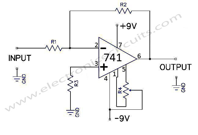
Fig.4. General Purpose Inverting DC Amplifier.
| PARTS LIST | |
| R1 | 10KΩ |
| R2 | 1MΩ |
| R3 | 10KΩ |
| R4 | 10KΩ |
A general purpose inverting type of dc amplifier operating on a dual symmetrical supply of ±9V is shown in Fig.4.
| INPUT Z | =R1 |
| 10KΩ | |
| GAIN | =R2/R1 |
| =100 | |
| BANDWIDTH | 1MHz/GAIN |
| 10KHz |
The input signal is applied to the inverting input terminal of the 741 and the output signal is therefore, phase inverted. The amplifier gain is decided by the ratio of the feedback resistors R1 and R2. The standing dc output voltage can be set exactly to zero by R4. The maximum output voltage swing is about ±7 volts.
2.NON -INVERTING DC AMPLIFIER

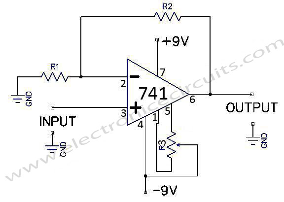
Fig.5. General Purpose Non-inverting DC Amplifier.
| PARTS LIST | |
| R1 | 1KΩ |
| R2 | 100KΩ |
| R3 | 10KΩ |
A general purpose non-inverting type of dc amplifier operating on a dual symmetrical supply of ±9V is shown in Fig.5.
| INPUT Z | >1MΩ |
| GAIN | 1+(R2/R1) |
| 101 | |
| BANDWIDTH | 1MHz/GAIN |
| 10KHz |
As before the gain of the amplifier is decided by the feedback resistor R1 and R2. Since the input signal is applied to the non-inverting input terminal of the 741, the output signal has the same phase as that of the input signal. The input impedance in this case is high but the signal source must provide a dc ground path for the input bias current. The standing output voltage can be set exactly to zero by R3. The output voltage swing is limited to approximately ±7 volts.
Please send your ideas, which are very important for our success…
I am always excited to visit this blog in the evenings.Please churning hold the contents. It is very entertaining.
WONDERFUL Post.thanks for share..more wait .. ;)…
Your place is valueble for me. Thanks!…
Super informative article, thanks a million.
These designs are really cool. I like this post Keep it up dude 🙂
Thank’s for your information abaut op amp 741 – 14 pin.
INTERESTING’
minta data ic yang 8 pin
Hello. I like electronics too.