555 Timer Time Delay Circuit
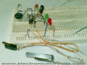
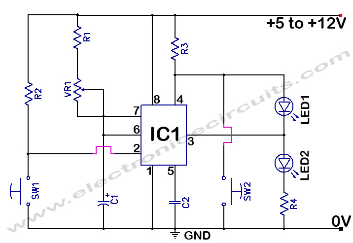
LEDs indicate at a glance what the status of the circuit is at any given moment. Once the reset switch, SW2, makes contact, the timer remains in that state until the start switch, S1, is pressed. When either switch is activated, LED1 (ready) and the time indicator, LED2, keep track of the situation.

| PARTS LIST | |
| R1 | 1KΩ |
| R2 | 10KΩ |
| R3 | 1KΩ |
| R4 | 1KΩ |
| VR1 | 1MΩ |
| C1 | 10µF |
| C2 | 0.01µF (103) |
| LED1 | GREEN LED (FOR READY) |
| LED2 | RED LED (FOR TIME) |
| IC1 | NE555 |
| SW1 | PUSH TO ON SWITCH (FOR START) |
| SW2 | PUSH TO ON SWITCH (FOR RESET) |
THE TIME DELAY, T, in seconds is:
T=1.1×C1×(R1+VR1)
The resistances are in megohms (MΩ) and capacitances in microfarads (µF).
The sum of R1 and VR1 should not be less than 1000Ω nor higher than 20MΩ.

Pressing S1 starts the timing cycle. A low-going pulse, instead of S1 can also be used to initiate the timing cycle. The output terminal, pin 3, of 555, is normally low and switches high during the timing cycle. The output can either sink or source currents up to 200mA. Therefore, a load such as a relay coil can be connected between pin3 and VCC or between pin 3 and ground, depending on circuit requirements. When the relay is connected between pin 3 and ground, it is normally de-energized so it is energized only during the timing cycle. Connecting the relay to ground will save power and allow the IC to run cool.
Please send your ideas, which are very important for our success…


Terrific work! This is the type of information that should be shared around the web. Shame on the search engines for not positioning this post higher!
thank you dude!!! you did an awesome job! The Best of the simplest circuits that i ever seen. . Easy to understand and explain. . .
any project display circuits we want them
realy its work and thax for share i think that you have to post these kind of knowledge good keep it up http://www.electronicecircuits.com
Thanks for the great post.
Awesome blog , thanks for the post!
I saw this really fantastic post today.Your blog post is very cogent and makes a number of great points.
Thank you so much!
Really worked and was perfect for the project I was doing – Turning a LED backlight on for a couple of seconds on button press.
Thanks again!
thank u so much..keep on sharing guys..GOD BLESSED YOU ALL..
Can you please explain what the right side of the schematic is doing? I am new to this and having difficulty deciphering the diagrams. Do the LEDs run one after the other in sequence? In what way are they connected to terminal 3 and 4 of the 555 IC? If mounting these on a breadboard, do the LEDs bridge over the gap between positive and negative side?
Note the path from Voltage in (+5 to +12v) goes through $3, then to both pin 4 and the anode (+) of LED1, then pin 3 connects between the two LEDs, and LED2 through R4 to ground. What happens is when pin 3 is high, the voltage across LED1 drops to minimal and LED1 is off, but the voltage across LED2 will be high, and it will therefore turn on. When pin 3 goes low, the opposite is true, so they switch which is illuminated.
I want ON time delay circuit 1 min delay i want and also i want mobile jammar circuit with out affecting bluthoot signal plz help me
i need best electronics technology with their components
I like this site.