Touch Volume Controlled Amplifier Circuit
Nowadays touch control techniques are becoming quite popular. They give better appearance to the control panel and are silent in operation. The circuit described here enables to control volume of the amplifier by simply touching corresponding touch pads. As there is no mechanical contact it is superior to the normal potentiometer type control. Its response is similar to the logarithmic response of human ears. It gives visual indication of the volume level by means of a single LED.

| PARTS LIST | |
| R1 | 2.2MΩ |
| R2 | 100KΩ |
| R3 | 100KΩ |
| R4 | 100KΩ |
| R5 | 1KΩ |
| R6 | 100Ω |
| R7 | 22Ω |
| R8 | 1Ω |
| R9 | 100KΩ |
| VR1 | 1KΩ |
| C1 | 2µF 250V POLYESTER |
| C2 | 470µF 10V |
| C3 | 0.1µF |
| C4 | 100µF 25V |
| C5 | 100µF 25V |
| C6 | 6.8Kp (6800pF) |
| C7 | 100µF 25V |
| C8 | 1000µF 25V |
| C9 | 1.5Kp (1500pF) |
| C10 | 0.1µF |
| D1 | LED |
| D2 | 5.1V 400mW |
| T1 | CD 4007 |
| T2 | |
| IC1 | TBA 810 |
| LS | 4Ω 20W |
| ABC | TOUCH PLATES |
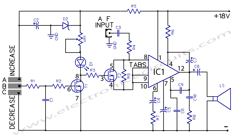
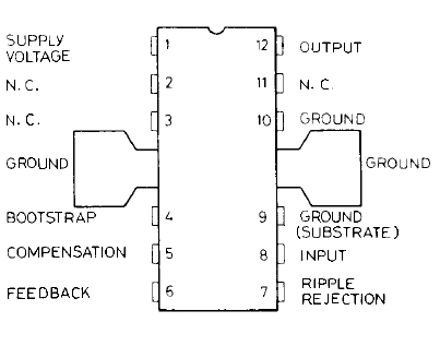
The heart of the circuit is a CMOSE IC CD4007 which comprises a dual complementary pair of MOSFETs and an inverter. It is not generally used in digital applications. Its Pin configuration is shown in Fig.2 and the complete circuit diagram of the system is shown in Fig.1. Two separate n-channel MOSFETs, T1 and T2, are used in this circuit. T2 acts as a voltage controlled attenuator and the control voltage is provided by T1. Gate to source voltage of T2 determines its drain to source resistance (Rds). It can be varied in the range of a few hundred ohms to several mega ohms.
 |  |
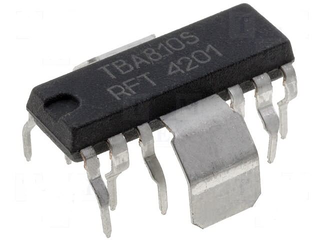
| TBA810 IC Top View | TBA810 Connection Diagram |
Now, consider the circuit operation. Initially there is no charge on C1 and Rds of T1 is maximum. So T2 gets full voltage and all the input signals appear across R4. Hence, the volume level of the amplifier is minimum. As C1 is charged by touching points A and B, the Rds of T1 decreases and volume increases as the control voltage of T2 decreases. Input resistance of T1 and T2 is of the order of 1012 ohms. So, the charge on capacitor C1 is hardly affected for an hour or two and the operation is stable.
Here IC1 is used as a power amplifier capable of delivering up to seven watts tms. However, for higher amplification any power amplifier having low input sensitivity may be used.

For setting VR1, short points A and D momentarily, provide input signal and adjust VR1 for maximum output. C1 should be a non-polarised polyester capacitor and its leakage current should be minimum. Gate and source (pin nos. 6 and 7) of T1 are physically close, so even dust particles will form discharge path for C1. This should be avoided. Finally, capacitor charging rate can be increased or decreased by changing the value of R1. It also depends upon personal touch and skin resistance.
Please send your ideas, which are very important for our success…
if u can provide PCB Layout. it more useful to us
thanks
please if you may send me all ele cir diag in past issu your sincerly eng a hamedi
For setting VR1, did you mean to say “short points A and C momentarily” instead of A and D?
The TBA 810 is a really old amp; wonder how this would work with more current amps.
This is a very nice linear application of a CMOS circuit, it would be nice if you could post more info about min and max input levels (like, for example, if it could work as a preamp stage –using an opamp instead of the TBA– for a guitar or microphone).
Must try it tomorrow!
Thanks!